Have you ever had to decide between a general purpose tool and one built for a very specific purpose? The general purpose tools can be used to solve many different problems, but may not be the best choice for any particular one. Purpose-built tools excel at one task, but you may need to do that particular task infrequently.
Computer engineers face this problem when designing architectures and instruction sets, almost always pursuing an approach that delivers good performance across a very wide range of workloads. From time to time, new types of workloads and working conditions emerge that are best addressed by custom hardware. This requires another balancing act: trading off the potential for incredible performance vs. a development life cycle often measured in quarters or years.
Enter the FPGA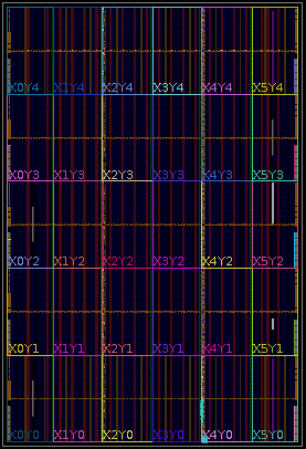 One of the more interesting routes to a custom, hardware-based solution is known as a Field Programmable Gate Array, or FPGA. In contrast to a purpose-built chip which is designed with a single function in mind and then hard-wired to implement it, an FPGA is more flexible. It can be programmed in the field, after it has been plugged in to a socket on a PC board. Each FPGA includes a fixed, finite number of simple logic gates. Programming an FPGA is “simply” a matter of connecting them up to create the desired logical functions (AND, OR, XOR, and so forth) or storage elements (flip-flops and shift registers). Unlike a CPU which is essentially serial (with a few parallel elements) and has fixed-size instructions and data paths (typically 32 or 64 bit), the FPGA can be programmed to perform many operations in parallel, and the operations themselves can be of almost any width, large or small.
This highly parallelized model is ideal for building custom accelerators to process compute-intensive problems. Properly programmed, an FPGA has the potential to provide a 30x speedup to many types of genomics, seismic analysis, financial risk analysis, big data search, and encryption algorithms and applications.
I hope that this sounds awesome and that you are chomping at the bit to use FPGAs to speed up your own applications! There are a few interesting challenges along the way. First, FPGAs have traditionally been a component of a larger, purpose-built system. You cannot simply buy one and plug it in to your desktop. Instead, the route to FPGA-powered solutions has included hardware prototyping, construction of a hardware appliance, mass production, and a lengthy sales & deployment cycle. The lead time can limit the applicability of FPGAs, and also means that Moore’s Law has time to make CPU-based solutions more cost-effective.
We think we can do better here!
The New F1 Instance
Today we are launching a developer preview of the new F1 instance. In addition to building applications and services for your own use, you will be able to package them up for sale and reuse in AWS Marketplace. Putting it all together, you will be able to avoid all of the capital-intensive and time-consuming steps that were once a prerequisite to the use of FPGA-powered applications, using a business model that is more akin to that used for every other type of software. We are giving you the ability to design your own logic, simulate and verify it using cloud-based tools, and then get it to market in a matter of days.
Equipped with Intel Broadwell E5 2686 v4 processors (2.3 GHz base speed, 2.7 GHz Turbo mode on all cores, and 3.0 GHz Turbo mode on one core), up to 976 GiB of memory, up to 4 TB of NVMe SSD storage, and one to eight FPGAs, the F1 instances provide you with plenty of resources to complement your core, FPGA-based logic. The FPGAs are dedicated to the instance and are isolated for use in multi-tenant environments.
Here are the specs on the FPGA (remember that there are up to eight of these in a single F1 instance):
- Xilinx UltraScale+ VU9P fabricated using a 16 nm process.
- 64 GiB of ECC-protected memory on a 288-bit wide bus (four DDR4 channels).
- Dedicated PCIe x16 interface to the CPU.
- Approximately 2.5 million logic elements.
- Approximately 6,800 Digital Signal Processing (DSP) engines.
- Virtual JTAG interface for debugging.
In instances with more than one FPGA, dedicated PCIe fabric allows the FPGAs to share the same memory address space and to communicate with each other across a PCIe Fabric at up to 12 Gbps in each direction. The FPGAs within an instance share access to a 400 Gbps bidirectional ring for low-latency, high bandwidth communication (you’ll need to define your own protocol in order to make use of this advanced feature).
The FPGA Development Process
As part of the developer preview we are also making an FPGA developer AMI available. You can launch this AMI on a memory-optimized or compute-optimized instance for development and simulation, and then use an F1 instance for final debugging and testing.
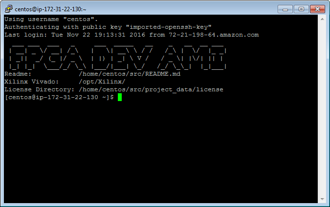
This AMI includes a set of developer tools that you can use in the AWS Cloud at no charge. You write your FPGA code using VHDL or Verilog and then compile, simulate, and verify it using tools from the Xilinx Vivado Design Suite (you can also use third-party simulators, higher-level language compilers, graphical programming tools, and FPGA IP libraries).
Here’s the Verilog code for a simple 8-bit counter:
module up_counter(out, enable, clk, reset);
output [7:0] out;
input enable, clk, reset;
reg [7:0] out;
always @(posedge clk)
if (reset) begin
  out <= 8'b0;
end else if (enable) begin
  out <= out + 1;
end
endmodule
Although these languages are often described as using C-like syntax (and that’s what I used to stylize the code), this does not mean that you can take existing code and recompile it for use on an FPGA. Instead, you need to start by gaining a strong understanding of the FPGA programming model, learn Boolean algebra, and start to learn about things like propagation delays and clock edges. With that as a foundation, you will be able to start thinking about ways to put FPGAs to use in your environment. If this is too low-level for you, rest assured that you can also use many existing High Level Synthesis tools, including OpenCL, to program the FPGA.
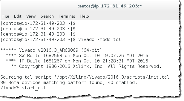
After I launched my instance, I logged in, installed a bunch of packages, and set up the license manager so that I could run the Vivado tools. Then I RDP’ed in to the desktop, opened up a terminal window, and started Vivado in GUI mode:
I opened up the sample project (counter.xpr) and was rewarded with my first look at how FPGA’s are designed and programmed:
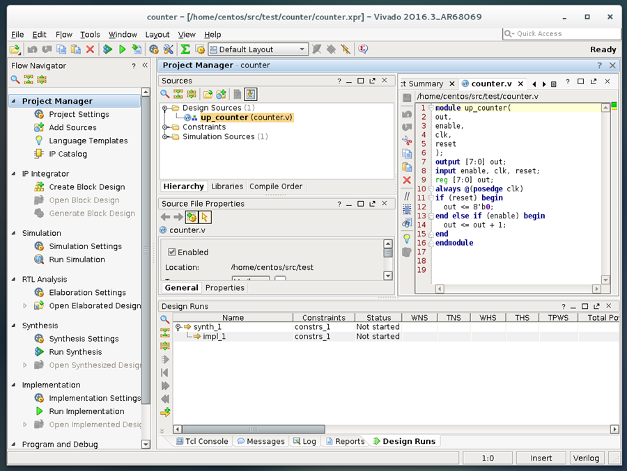
After a bit of exploration I managed to synthesize my first FPGA (I was doing little more than clicking interesting stuff at this point; I am not even a novice at this stuff):
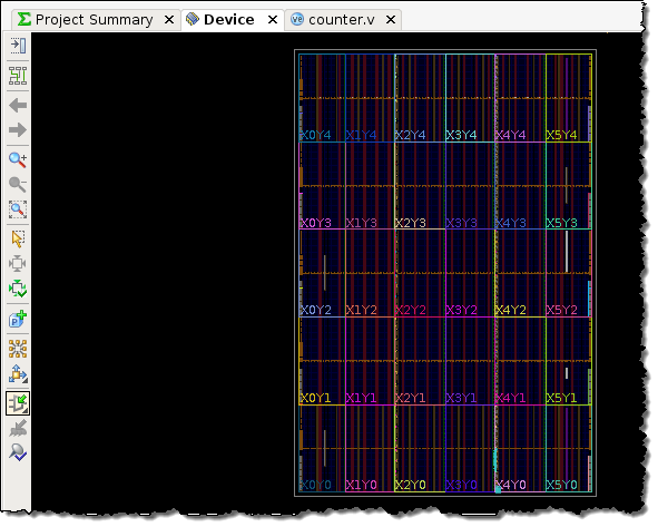
From here, I would be able to test my design, package it up as an Amazon FPGA Image (AFI), and then use it for my own applications or list it in AWS Marketplace. I hope to be able to show you how to do all of these things within a couple of weeks.
The F1 Hardware Development Kit
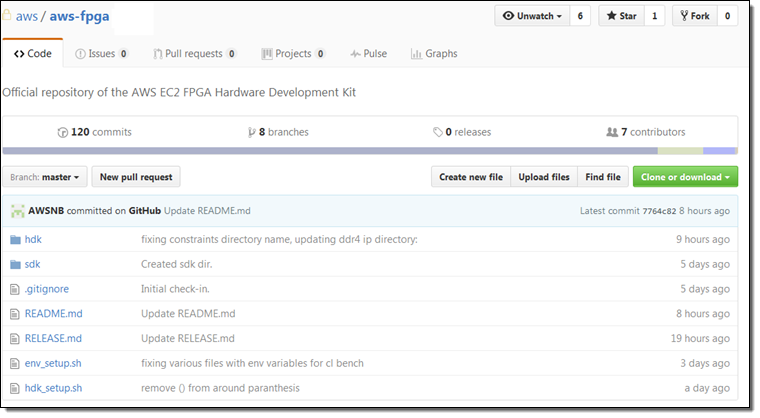
After I learned about the F1 instances, one of my first questions had to do with the interfaces between the FPGA(s), the CPU(s), and main memory. The F1 Hardware Development Kit (HDK) includes preconfigured I/O interfaces and sample applications for multiple communication methods including host-to-FPGA, FPGA-to-memory, and FPGA-to-FPGA. It also includes compilation scripts, reference examples, and an in-field debug toolset.
The Net-Net
The bottom line here is that the combination of the F1 instances, the cloud-based development tools, and the ability to sell FPGA-powered applications is unique and powerful. The power and flexibility of the FPGA model is now accessible all AWS users; I am sure that this will inspire entirely new types of applications and businesses.
Get Started Today
As I mentioned earlier, we are launching in developer preview form today in the US East (Northern Virginia) Region (we will expand to multiple regions when the instances become generally available in early 2017). If you have prior FPGA programming experience and are interested in getting started, you should sign up now.
— Jeff;
